3. YBCO thin film growth
- an original YBCO deposition method was proposed
- the YBCO thin film was grown using the Chemical Solution Deposition (CSD) technique
- the fluorine free coating solution was prepared using cost effective metal acetate precursors Y(CH3COO)3 ·4H2O, Ba(CH3COO)2, Cu(CH3COO)2 in a stoichiometric ratio Y3+: Ba2+: Cu2+ = 1:2:3
- 10% vol. of diethanolamine (DEA) was added to improve the solution viscosity and stability
- thermal treatment:
- 600 °C with a dwell time of 60 minutes, in humid O2 flow (20 l/hour) - pyrolisis.
- 835 °C at a heating rate of 20 °C/min, for 180 min in a humid N2/O2 atmosphere - crystallization
- 450 °C, 1 hour in an oxygen flow - oxygenation step
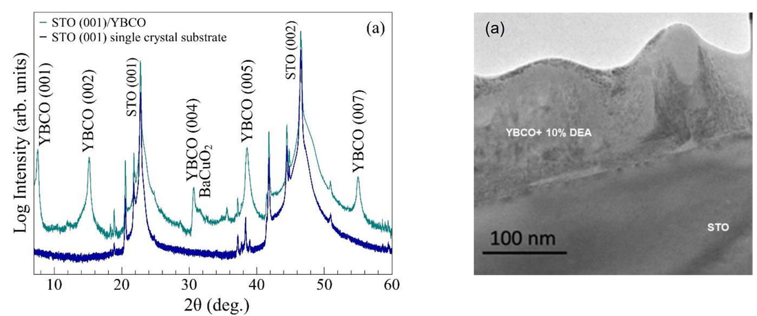
- X-ray diffraction confirms the epitaxial growth of YBCO, while transmission electron microscopy investigations show a film thickness of approx. 100 nm (both shown below)
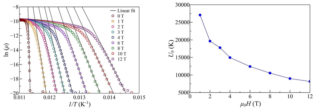
- zero-resistance critical temperature, Tc(R=0) is 88.1 K
- to calculate the pinning energy, U0, the ρ(T) data is plotted in an Arrhenius form ln(ρ) vs. 1/T and fitted according to the thermally activated flux-flow (TAFF) expression (shown below)
- good agreement was found between the calculated U0 values and other repots found in literature, demonstrating that the proposed method is suitable for high-quality YBCO thin film growth
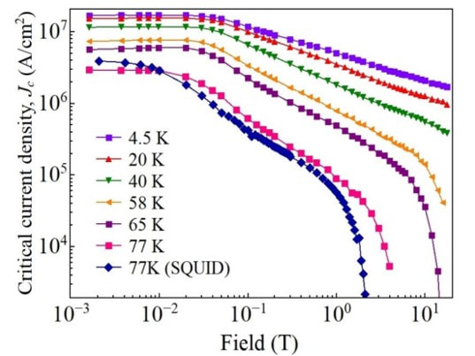
- transport measurements reveal a critical current density, Jc, value in self-field of 3 MA/cm^2
- maximum pinning force density, Fp,max, was 0.95 GN/m^3 , determined from transport measurements
- low irreversibility field value, Hirr = 2.2 T (determined as the field at which the normalized pinning force decrease below 0.01)
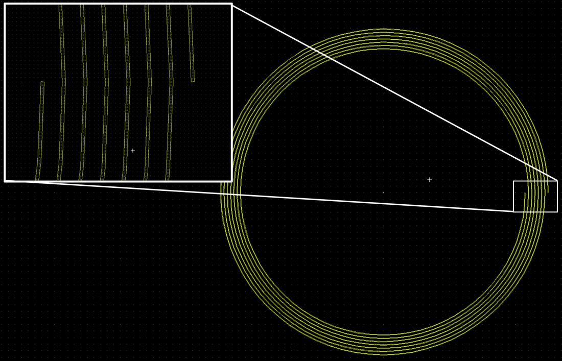
RF coil UV lithography mask design
- for the fabrication of the RF coil a UV lithography mask design was developed using the LayoutEditor software (shown below)
- the mask uses a standard multi-turn receiver coil geometry:
- 8 turns
- 150 µm width/turn
- outer diameter of the coil is 20 mm
- inner diameter is 17 mm